
Company News
Company News
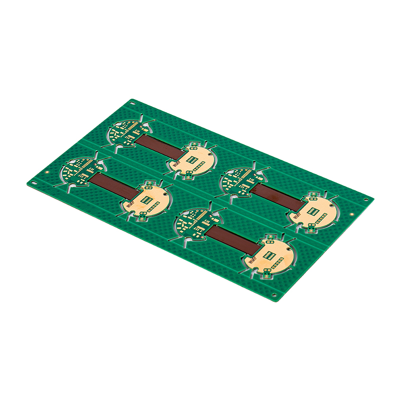
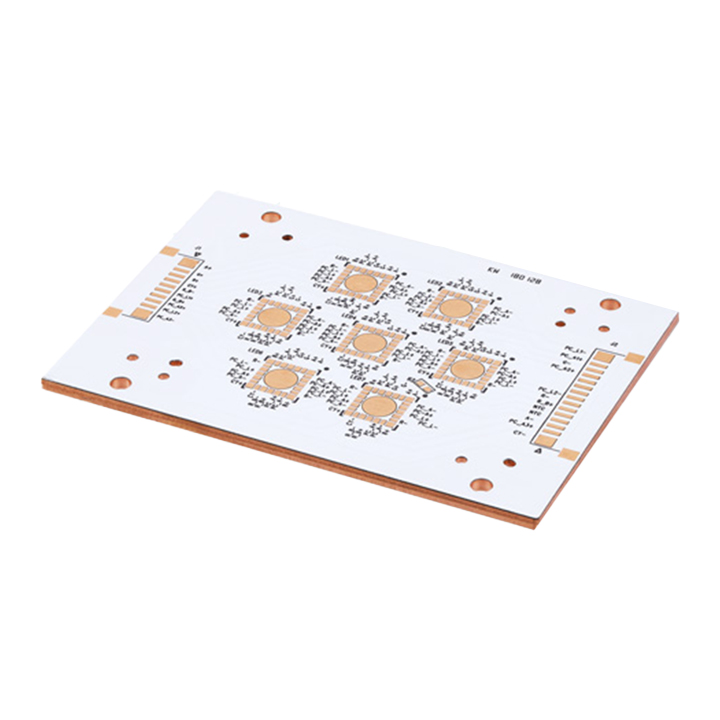
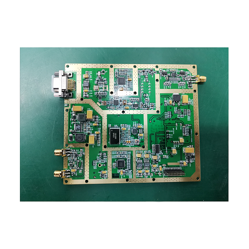
Password Decryption for PCB Circuit Board Design: Key Points for Layout and Wiring
Author:Suclink
Release Time:2025-11-21
Page Views:65
For circuit board engineers, mastering the key points of layout and wiring is like unlocking the password for circuit board design.
At the beginning of the layout, it is necessary to clarify the core functional modules. Based on the signal flow and functional logic, gradually radiate and layout other components outward. Shorten the signal transmission path, reduce transmission delay and loss. At the same time, it is necessary to fully consider the heat dissipation requirements of the components. For components with high heat generation, specialized heat dissipation channels can be set up if necessary to prevent heat accumulation from affecting the normal operation of the circuit board.
The wiring process also tests the skills of engineers. The primary principle is to maintain signal integrity. High frequency signals are extremely sensitive to line length and impedance matching, so it is important to make high-frequency lines as short and straight as possible, avoiding sharp angles and right angle turns, in order to reduce signal reflection and interference. For differential signal pairs, the two lines must be strictly of equal length to ensure synchronous signal transmission. In multi-layer circuit boards, it is also crucial to plan different signal layers reasonably. The power layer, ground layer, and signal layer should be layered to reduce interlayer interference. The power wiring needs to be thick enough to carry high currents and prevent the circuit from overheating and burning out.
In addition, electromagnetic compatibility (EMC) cannot be ignored. Components that are susceptible to interference, such as sensitive analog circuit parts, should be kept away from interference sources, such as high-power digital chips, switching power supplies, etc. Electromagnetic interference can be controlled within a safe range by adding shielding covers and setting grounding appropriately. At the same time, sufficient space should be reserved at the edge of the circuit board for setting grounding frames, further enhancing anti-interference capabilities.
Hot News
-
 Why do PCB circuit boards need to be gold-plated and gold-plated2025-11-21
 -
 What is the appropriate thickness for gold deposition on circuit boards2025-11-21
 -
 How does a circuit board affect the performance of electronic devices?2025-11-21
 -
 Password Decryption for PCB Circuit Board Design: Key Points for Layout and Wiring2025-11-21